📑Table of Contents:
- What Is a Scanning Microscope?
- Materials Science and Failure Analysis
- Electronics and Semiconductor Inspection
- Biology and Life Science Research
- Medical and Biomedical Applications
- Forensic Science
- Geology, Minerals, and Environmental Science
- Nanotechnology and Advanced Materials
- Quality Control and Manufacturing
- Art, Archaeology, and Cultural Heritage
- Limitations of Scanning Microscopes
- Final Thoughts

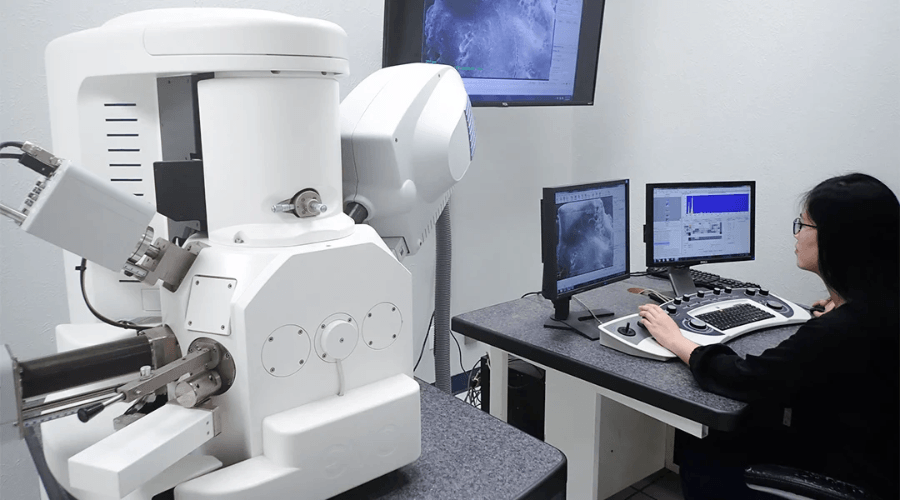
Scanning microscopes cover a wide range of fields, from materials science and biology to electronics, manufacturing, forensics, geology, and nanotechnology. In most cases, people use the phrase “scanning microscope” to refer to a scanning electron microscope, or SEM. An SEM scans a sample with a focused electron beam and creates detailed images from signals released by the sample surface. As a result, it can show tiny structures that ordinary light microscopes cannot reveal.
However, an SEM does more than make impressive close-up pictures. It helps researchers measure surface texture, identify defects, compare materials, study cells, inspect microchips, analyze particles, and investigate failures. Additionally, when paired with energy-dispersive X-ray spectroscopy, or EDS/EDX, it can help identify which elements exist in a sample. Therefore, scanning microscopes have become essential tools wherever surface detail and microscopic evidence matter.
What Is a Scanning Microscope?
A scanning microscope forms an image by moving a focused beam across a sample point by point. In a scanning electron microscope, the beam consists of electrons rather than visible light. When the electrons hit the sample, they produce signals such as secondary electrons, backscattered electrons, and X-rays. Then, detectors collect those signals, and a computer builds an image.
This scanning process gives SEM two major advantages. First, it can reveal very fine surface detail. Second, it offers strong depth of field, so rough or three-dimensional surfaces often look sharply focused. The University of Melbourne’s microscopy learning materials note that electron microscopes can reach much higher resolution than light microscopes and that SEM can maintain high resolution with good depth of field. Consequently, SEM works especially well for textured, fractured, rough, or tiny samples.
Because SEM focuses mainly on surfaces and near-surface regions, it does not replace every microscope. However, when surface structure matters, few tools provide the same level of detail.
Materials Science and Failure Analysis
Materials science is one of the most important areas for the use of scanning microscopes. Researchers and engineers use SEM to study metals, ceramics, polymers, composites, coatings, powders, fibers, and nanomaterials. They can inspect grain structure, fracture surfaces, corrosion, wear patterns, cracks, voids, inclusions, and surface roughness.
For example, if a metal part fails, SEM can help determine whether it fractured due to fatigue, overload, corrosion, or manufacturing defects. The fracture surface may show tiny ridges, dimples, brittle cleavage features, or crack origins. Additionally, EDS can identify contaminants or unexpected elements near the failure point.
This matters for aircraft parts, medical implants, automotive components, pipelines, batteries, construction materials, and industrial equipment. Thermo Fisher describes SEM as valuable for quality assurance, quality control, cleanliness compliance, and materials applications. Therefore, SEM helps companies not only understand what went wrong but also prevent repeat failures.
Electronics and Semiconductor Inspection
Electronics manufacturing depends heavily on microscopic inspection. Modern circuits, sensors, microelectromechanical systems, and semiconductor devices contain features far smaller than the eye can see. Therefore, scanning microscopes help engineers inspect chip structures, solder joints, thin films, coatings, contacts, defects, contamination, and fabrication problems.
SEM can show broken traces, particles, voids, delamination, surface damage, or patterning errors. Additionally, EDS can help identify whether a particle contains silicon, copper, aluminum, tin, gold, or other elements. This makes SEM useful for troubleshooting production lines and improving yield.
Moreover, as electronic devices shrink, inspection tools must provide higher resolution. Recent research continues to explore SEM-linked nanoscale imaging methods for integrated circuits and advanced materials. Consequently, scanning microscopy remains central to electronics development, reverse engineering, quality control, and failure analysis.
Biology and Life Science Research
Scanning microscopes also play a major role in biology. Life scientists use SEM to study cells, tissues, plants, insects, pollen, bacteria, parasites, organs, biofilms, and biomaterials. Unlike a light microscope, which often reveals transparent or stained internal structures, SEM excels at revealing surface morphology and ultrastructure.
ZEISS explains that SEM in life science research can provide topographical imaging, compositional studies, and 3D reconstruction of ultrastructure. It also notes that SEM can image biological surface structures and support large-field, high-resolution imaging. This makes it useful for studying insect eyes, leaf stomata, cell surfaces, tissue architecture, and microscopic organisms.
However, biological samples often require preparation because conventional SEM operates under vacuum conditions. Researchers may fix, dehydrate, dry, coat, or freeze samples before imaging. Additionally, low-vacuum, environmental, cryo-, and volume SEM methods can expand what researchers can study. Therefore, biology uses SEM not just for beautiful images, but for structural evidence that supports real scientific questions.
Medical and Biomedical Applications
Medical and biomedical researchers use scanning microscopes to study implants, tissue scaffolds, drug delivery particles, dental materials, bone surfaces, biofilms, surgical devices, and cell-material interactions. For example, a researcher might use SEM to see how cells attach to a titanium implant surface or how a scaffold’s pores support tissue growth.
Additionally, SEM helps evaluate medical-device surfaces. Tiny scratches, residues, coatings, or manufacturing defects can affect performance. In dentistry, SEM can reveal enamel surfaces, filling materials, dentin tubules, adhesive interfaces, and implant coatings. In biomaterials research, it can help compare roughness, porosity, and degradation.
Moreover, SEM combined with EDS can identify mineral deposits, inorganic particles, or elemental composition in biomedical samples. As a result, it supports both research and quality checks in healthcare-related manufacturing.
Forensic Science
Forensic labs use scanning microscopes when tiny evidence matters. SEM can help compare fibers, paint chips, glass fragments, soil particles, tool marks, gunshot residue, and unknown debris. Because SEM reveals surface texture at high magnification, it can show details that help analysts compare whether materials may share a common origin.
Forensic SEM often pairs with EDS. Gunshot residue analysis, for example, may look for characteristic particles containing elements such as lead, barium, and antimony, depending on ammunition type and modern lead-free alternatives. Additionally, SEM can support the investigation of explosives residues, industrial particles, and trace evidence.
EBSCO’s forensic overview describes SEM as a powerful imaging technique for comparing materials and revealing detailed surface characteristics that may indicate common origin. Therefore, forensic SEM helps turn microscopic fragments into useful investigative information.
Geology, Minerals, and Environmental Science
Geologists and environmental scientists use SEM to study minerals, rocks, sediments, fossils, volcanic ash, soils, microplastics, and atmospheric particles. SEM can reveal crystal shapes, weathering patterns, pore structures, mineral boundaries, and tiny inclusions. Additionally, EDS can identify elemental composition, which helps researchers interpret mineral phases and contamination sources.
For example, SEM can help analyze sand grains, clay minerals, ore samples, meteorites, or industrial dust. Environmental researchers may use it to examine particulate matter, filter residues, or microplastic surfaces. Moreover, paleontologists can use SEM to inspect fossil textures, tiny shells, or preserved microstructures.
Because many geological samples have rough surfaces and mixed compositions, SEM’s depth of field and elemental analysis capabilities make it especially valuable.
Nanotechnology and Advanced Materials
Nanotechnology depends on tools that can see and measure extremely small structures. Scanning microscopes help researchers examine nanoparticles, nanofibers, nanotubes, thin films, catalysts, membranes, coatings, and 3D-printed microstructures. SEM can show particle size, shape, distribution, agglomeration, surface roughness, and defects.
Recent reviews of nanomaterials research describe SEM and TEM as essential characterization tools for nanoscale and atomic-scale investigation. SEM matters because many nanoscale properties depend on morphology. A nanoparticle’s shape, coating, clustering, or surface texture can change how it behaves in electronics, medicine, energy storage, filtration, and catalysis.
Therefore, scanning microscopes support innovation in batteries, solar cells, sensors, drug delivery, coatings, and advanced manufacturing.
Quality Control and Manufacturing
Manufacturers use SEM to improve products and monitor processes. In quality control, it can inspect raw materials, powders, coatings, fibers, machined parts, filters, seals, and packaging. It can also detect contamination that standard visual inspection misses.
For example, a company might use SEM to examine why a coating peeled, why a plastic part cracked, or why a powder clumped. Additionally, SEM can support cleanliness testing by identifying particles on components that must meet strict contamination standards.
This role matters in aerospace, automotive, pharmaceuticals, electronics, energy, and medical devices. When a defect is too small for a standard microscope, SEM can provide evidence to guide process improvements.
Art, Archaeology, and Cultural Heritage
Scanning microscopes also help museums, conservators, and archaeologists. SEM can examine pigments, corrosion layers, ceramics, metals, fibers, paper, bones, shells, and tool marks. Additionally, EDS can help identify elements in pigments, glazes, alloys, or residues.
For example, conservators may study paint layers on an artifact without destroying the whole object. Archaeologists may compare pottery surfaces or examine wear patterns on tools. Moreover, SEM can help identify degradation processes, which supports better preservation.
Although this field may seem far from engineering, the goal remains similar: use microscopic evidence to understand materials, history, and change over time.
Limitations of Scanning Microscopes
Scanning microscopes have limits. SEM usually needs vacuum-compatible samples, and non-conductive materials may need coating or low-vacuum methods. Wet biological samples can require special preparation. Additionally, SEM images usually appear in grayscale unless someone adds false color later.
The University of Melbourne notes several limitations, including vacuum compatibility, dehydration requirements for some samples, challenges with insulating materials, added preparation steps, and the fact that SEM is mainly a surface-scanning technique. Therefore, users must choose SEM only when it is appropriate for the question.

Final Thoughts
Scanning microscopy spans materials science, electronics, biology, medicine, forensics, geology, environmental science, nanotechnology, manufacturing, and cultural heritage. SEM helps users see surface detail, compare structures, identify defects, study biological form, analyze tiny particles, and support quality control. Additionally, EDS can add elemental information that turns images into richer material evidence.
Ultimately, scanning microscopes matter because they reveal the hidden surfaces of the world. They show why a part failed, how a cell looks, what a particle contains, or how a material behaves at tiny scales. When researchers, engineers, and analysts need answers beyond the reach of ordinary light microscopes, scanning microscopy gives them a sharper way to investigate.