📑Table of Contents:
- What Is a Scanning Electron Microscope?
- How Does a Scanning Electron Microscope Work?
- What Are the Main Parts of an SEM?
- What Do SEM Detectors Actually Measure?
- How Powerful Is a Scanning Electron Microscope?
- Why Does an SEM Need a Vacuum?
- How Are Samples Prepared for SEM Imaging?
- What Is the Difference Between SEM and TEM?
- What Is Scanning Electron Microscopy Used For?
- What Are the Advantages of an SEM?
- Can a Scanning Electron Microscope See Atoms?
- Scanning Electron Microscope Explained in Simple Answer

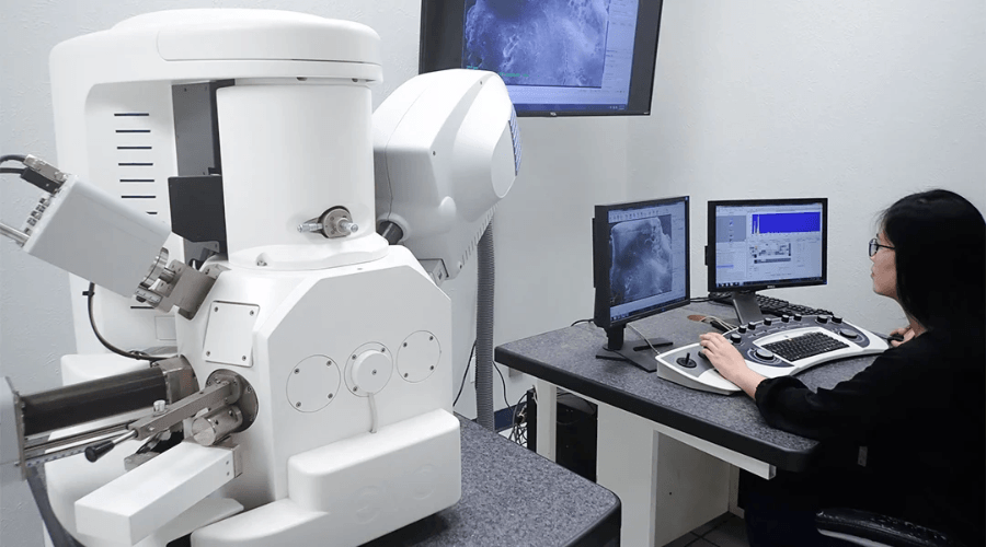
A scanning electron microscope, or SEM, is a powerful scientific instrument that uses a focused electron beam to create highly detailed images of a specimen’s surface. Unlike an ordinary light microscope, an SEM does not illuminate a sample with visible light. Instead, it scans electrons across the specimen and measures the signals produced by their interaction with the material.
As a result, scientists can examine structures far smaller than those visible through conventional optical microscopes. Moreover, SEM images reveal fine surface textures, fractures, particles, biological structures, and material differences with impressive clarity.
Today, researchers use scanning electron microscopy across medicine, engineering, electronics, geology, materials science, manufacturing, and many other fields.
What Is a Scanning Electron Microscope?
A scanning electron microscope creates magnified images by directing electrons toward a sample and scanning them systematically across its surface.
When those electrons hit the specimen, several interactions occur. As a result, the sample releases or reflects different signals. Detectors collect these signals, and computer software converts them into an image.
Most SEM images appear in grayscale rather than natural color. However, researchers can add artificial colors afterward to highlight particular structures or materials.
Furthermore, an SEM often produces images with a striking three-dimensional appearance because it offers a large depth of field. This quality makes rough surfaces, tiny particles, insects, metals, and microscopic structures especially dramatic.
How Does a Scanning Electron Microscope Work?
An SEM works through a sequence of carefully controlled steps.
First, an electron source at the top of the microscope generates electrons. Depending on the instrument, the source may use a tungsten filament, lanthanum hexaboride crystal, or field-emission technology.
Next, an electrical field accelerates the electrons down the microscope column. Electromagnetic lenses then focus them into a very narrow beam.
Afterward, scanning coils move the beam across the specimen in a raster pattern. In simple terms, the beam travels across the surface line by line, much like a television or computer display builds an image from many individual points.
Meanwhile, every location produces signals when the beam interacts with the material. Detectors measure their intensity and send the data to a computer.
Finally, the computer assigns brightness values to those signals and builds the SEM image pixel by pixel.
Therefore, an SEM does not take a photograph in the traditional sense. Instead, it constructs an image from measurements collected while electrons scan the sample.
What Are the Main Parts of an SEM?
Although modern instruments vary in design, most scanning electron microscopes contain several essential components.
The electron gun generates the primary electron beam. Meanwhile, electromagnetic lenses and apertures shape and focus that beam.
Scanning coils control where the beam lands on the specimen. Additionally, the sample sits on a movable stage inside a specimen chamber, allowing the operator to reposition or tilt it.
Detectors collect signals produced during electron-sample interactions. Finally, a vacuum system removes most gas molecules from the microscope column and chamber.
The major components include:
- Electron source or electron gun
- Electromagnetic lenses
- Apertures
- Scanning coils
- Specimen chamber
- Sample stage
- Electron detectors
- X-ray detector on equipped systems
- Vacuum system
- Computer and control software
Together, these parts allow researchers to control magnification, focus, contrast, beam energy, and image composition.
What Do SEM Detectors Actually Measure?
An electron beam produces several types of signals when it hits a specimen. However, secondary electrons and backscattered electrons provide two of the most important imaging signals.
Secondary electrons escape from regions close to the sample surface. Therefore, they provide excellent information about surface shape and texture.
For example, secondary-electron imaging can reveal tiny cracks, ridges, fibers, pores, and particles.
Backscattered electrons work differently. Some incoming electrons collide with atoms and travel back out of the specimen. Furthermore, heavier elements generally backscatter more electrons than lighter ones.
As a result, backscattered-electron images can show compositional differences. Areas containing elements with higher atomic numbers often appear brighter.
Additionally, electron interactions can produce characteristic X-rays. When an SEM includes energy-dispersive X-ray spectroscopy, or EDS/EDX, researchers can analyze these X-rays to identify elements in the sample.
Therefore, an SEM can reveal much more than surface appearance alone.
How Powerful Is a Scanning Electron Microscope?
SEM performance depends on the instrument, electron source, specimen, operating conditions, and imaging method.
Nevertheless, scanning electron microscopes can resolve structures on the nanometer scale. Advanced field-emission SEM systems can achieve sub-nanometer resolution under suitable conditions.
By comparison, conventional light microscopes face fundamental resolution limits because they rely on visible wavelengths.
Therefore, an SEM can reveal structures that an optical microscope cannot clearly distinguish.
However, magnification and resolution are not the same thing. Enlarging an image does not automatically reveal additional detail. Instead, resolution describes how well the microscope can distinguish two extremely close features.
Consequently, resolution provides a more meaningful measure of SEM imaging power than magnification alone.
Why Does an SEM Need a Vacuum?
Electrons do not travel efficiently through ordinary air.
If many gas molecules remained inside the microscope, electrons would collide with them before reaching the sample. As a result, those collisions scatter the beam and reduce image quality.
A vacuum therefore creates a controlled path between the electron source and the specimen.
Moreover, the vacuum helps maintain stable conditions around sensitive electron-optical components.
Some specialized low-vacuum or variable-pressure SEM systems can operate with more gas inside the specimen chamber. As a result, they can examine certain samples that would prove difficult to study under conventional high-vacuum conditions.
How Are Samples Prepared for SEM Imaging?
Sample preparation depends heavily on the material.
Conductive materials such as many metals often require relatively little preparation. However, nonconductive materials can accumulate electrical charge when exposed to the electron beam.
Consequently, researchers often cover these specimens with an extremely thin conductive coating. Common coating materials include carbon, gold, platinum, or metal alloys.
Biological samples may require additional preparation. For instance, researchers commonly need to preserve and dry tissues before conventional SEM examination.
Furthermore, preparation must preserve the features that researchers want to study. An excessively thick coating could hide extremely fine surface structures.
Therefore, good sample preparation plays a major role in obtaining reliable SEM images.
What Is the Difference Between SEM and TEM?
Scanning electron microscopy and transmission electron microscopy both use electrons, but they examine samples differently.
| Feature | SEM | TEM |
|---|---|---|
| Main information | Surface and near-surface | Internal structure |
| Electron behavior | Scans specimen surface | Passes through thin specimen |
| Typical appearance | 3D-like surface image | 2D internal projection |
| Sample preparation | Often simpler | Usually more demanding |
| Depth of field | High | Lower for conventional images |
| Common uses | Surfaces, particles, fractures | Cells, crystals, nanostructures |
Therefore, researchers usually choose SEM when surface morphology matters most. In contrast, TEM becomes valuable when they need to investigate structures inside an extremely thin specimen.
What Is Scanning Electron Microscopy Used For?
SEM has become valuable across an enormous range of scientific and industrial applications.
Materials scientists use it to examine metals, ceramics, polymers, coatings, and composite materials. Similarly, engineers inspect fractures to determine why components failed.
Semiconductor manufacturers can investigate extremely small electronic structures and manufacturing defects. Meanwhile, geologists examine minerals and microscopic rock structures.
Biologists also use SEM to study insects, pollen, microorganisms, teeth, bones, tissues, and plant surfaces.
Other Applications Include:
- Nanotechnology research
- Battery development
- Pharmaceutical analysis
- Forensic investigations
- Failure analysis
- Quality control
- Aerospace engineering
- Automotive manufacturing
- Microelectronics
- Additive manufacturing
Therefore, SEM serves both fundamental research and practical industrial problem-solving.
What Are the Advantages of an SEM?
One major advantage is extremely detailed surface imaging.
Additionally, SEM offers a much greater depth of field than ordinary optical microscopy, which creates clear images of uneven samples.
Researchers can also examine relatively large areas before zooming into microscopic features. Furthermore, instruments equipped with analytical detectors can provide elemental composition information.
However, SEM also has limitations. Conventional instruments require a vacuum, and some specimens need significant preparation. Moreover, electron beams can damage sensitive materials.
SEM images also lack natural color because electron detectors measure signal intensity rather than visible wavelengths.
Finally, high-performance systems can cost considerably more than ordinary optical microscopes and require trained operators.
Can a Scanning Electron Microscope See Atoms?
A conventional SEM does not normally produce clear images of individual atoms.
Instead, SEM excels at visualizing surfaces and structures from micrometer scales down into the nanometer range. Advanced field-emission instruments can achieve extremely high resolution, but scientists generally rely on specialized TEM, or scanning transmission electron microscopy, when true atomic-scale imaging is necessary.
Therefore, statements claiming that every SEM can “see atoms” oversimplify its capabilities.

Scanning Electron Microscope Explained in Simple Answer
A scanning electron microscope uses a focused electron beam to scan a specimen and measure signals created by electron-material interactions.
Secondary electrons reveal surface detail, while backscattered electrons can highlight compositional differences. Additionally, characteristic X-rays can identify elements when the microscope includes suitable analytical equipment.
Unlike a light microscope, an SEM relies on electrons, electromagnetic lenses, detectors, and usually a vacuum environment. As a result, it can resolve remarkably small surface features while producing images with excellent depth of field.
Ultimately, scanning electron microscopy lets scientists investigate a world that remains invisible to the naked eye. From microscopic cracks in aircraft components to the intricate surface of pollen grains, SEM technology turns nanoscale structures into information researchers can see, measure, and understand.