📑Table of Contents:
- What Is a Scanning Electron Microscope?
- Why SEM Uses Electrons Instead of Light
- The Main Parts of an SEM
- Step 1: Creating the Electron Beam
- Step 2: Scanning the Sample Surface
- Step 3: Electron-Sample Interactions
- Step 4: Detecting the Signals
- Step 5: Building the Image
- Why Samples Need Preparation
- SEM vs. Light Microscope
- Final Thoughts

A scanning electron microscope, or SEM, uses a focused beam of electrons rather than visible light to examine the surface of a sample. Because electrons have much shorter wavelengths than visible light, an SEM can reveal details far smaller than a standard optical microscope can show. As a result, scientists, engineers, forensic analysts, materials researchers, and biologists use SEMs to study textures, fractures, cells, metals, ceramics, polymers, microchips, powders, insects, fibers, and countless other tiny structures.
However, an SEM does not work like a camera that simply “takes a picture.” Instead, it scans the sample point by point. At each location, the electron beam interacts with the material, producing signals. Then, detectors collect those signals, and a computer turns them into an image. Therefore, the final SEM image represents a map of electron interactions, not a normal photograph.
What Is a Scanning Electron Microscope?
A scanning electron microscope forms images by scanning a sample surface with a narrow electron beam. Unlike a light microscope, which uses lenses to focus visible light, an SEM uses electromagnetic lenses to focus electrons. Additionally, it needs a vacuum chamber because electrons scatter easily in air.
The word “scanning” matters. The microscope does not illuminate the whole sample at once. Instead, it moves the beam across the surface in a raster pattern, similar to how old television screens built images line by line. At every point, the sample releases or reflects electrons. The SEM records the signal strength and assigns a brightness value to each point in the image.
Consequently, SEM images often look highly detailed and three-dimensional. They show surface shape, edges, roughness, particles, cracks, pores, grains, and tiny structures with dramatic depth.
Why SEM Uses Electrons Instead of Light
SEM uses electrons because electrons can reveal much smaller details than visible light. In optical microscopes, resolution is limited because light waves have wavelengths on the order of hundreds of nanometers. Electron beams can behave with much shorter wavelengths, so they can resolve much finer structures.
This does not mean every SEM image reaches atomic detail. Resolution depends on beam size, sample preparation, detector type, vibration, charging, working distance, and operating voltage. However, modern SEMs can achieve nanometer-scale detail under the right conditions. ZEISS explains that SEMs use high-energy electrons rather than visible light to scan a specimen and can reach much higher resolving power than standard light microscopes.
Moreover, electrons do more than form images. When they strike the sample, they can produce secondary electrons, backscattered electrons, and X-rays. Each signal gives different information, so SEM can combine surface imaging with material analysis.
The Main Parts of an SEM
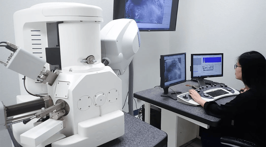
A scanning electron microscope contains several important parts. First, an electron source generates electrons. This source may use a tungsten filament, a lanthanum hexaboride crystal, or a field emission gun. Next, electromagnetic lenses focus the electrons into a narrow beam.
Then, scanning coils move the beam across the sample. The sample sits on a stage inside a vacuum chamber, where the operator can move, tilt, rotate, or raise it. Detectors collect signals from the sample, and a computer converts those signals into an image.
The Main Parts Include:
- Electron gun
- Condenser lenses
- Objective lens
- Scanning coils
- Apertures
- Vacuum chamber
- Sample stage
- Secondary electron detector
- Backscattered electron detector
- X-ray detector when chemical analysis is needed
- Computer and imaging software
Together, these parts control the electron beam, collect information, and build the final SEM image.
Step 1: Creating the Electron Beam
The process starts in the electron gun. The gun emits electrons and accelerates them down the microscope column with an applied voltage. This accelerating voltage can vary depending on the sample and imaging goal. Higher voltages can penetrate deeper and produce stronger signals, while lower voltages can reduce charging and improve surface sensitivity for delicate samples.
After the gun releases electrons, electromagnetic lenses shape and narrow the beam. Unlike glass lenses in light microscopes, SEM lenses use magnetic fields to control electron paths. The microscope also uses apertures to refine the beam and reduce the number of unwanted electrons.
Because the beam must stay narrow and stable, the SEM column needs careful alignment. If the beam spreads too much, the image loses sharpness. Therefore, operators adjust focus, astigmatism, aperture settings, and working distance to improve image quality.
Step 2: Scanning the Sample Surface
Once the microscope forms a focused beam, scanning coils move it across the sample surface. The beam travels point by point in a grid. At each point, electrons enter or strike the sample and interact with its atoms.
This scanning pattern creates the image gradually. The detector measures the signal intensity from each beam position. Then, the computer places a matching brightness value at the corresponding point on the screen. A stronger signal may appear brighter, while a weaker signal may appear darker.
Additionally, scan speed affects image quality. A fast scan can help the operator navigate quickly, but it may look noisy. A slower scan collects more signal at each point and often creates a cleaner image. Therefore, operators often use fast scans for searching and slower scans for final images.
Step 3: Electron-Sample Interactions
When the electron beam hits the sample, several types of signals can emerge. Thermo Fisher explains that SEMs commonly detect secondary electrons, backscattered electrons, and characteristic X-rays, all of which can help build images or analyze chemical structure.
Secondary electrons come from atoms near the sample surface. Because they originate close to the surface, they provide excellent surface detail. They help reveal texture, edges, fine particles, pores, and topography.
Backscattered electrons are primary beam electrons that bounce back after interacting with sample atoms. These electrons often carry composition information because heavier elements tend to backscatter more strongly than lighter elements. Therefore, backscattered electron images can show material contrast, such as different phases in a metal alloy.
Characteristic X-rays are emitted when the beam knocks inner-shell electrons out of atoms, and higher-energy electrons drop down to fill the vacancies. This process emits X-rays with energies characteristic of specific elements. Consequently, SEMs equipped with energy-dispersive X-ray spectroscopy (EDS/EDX) can identify elements in the sample.
Step 4: Detecting the Signals
Detectors collect the signals that leave the sample. The secondary electron detector typically captures low-energy electrons emitted from the surface, producing detailed images with high topographic contrast. Meanwhile, a backscattered electron detector captures higher-energy reflected electrons, often highlighting compositional differences.
Thermo Fisher notes that secondary electrons and backscattered electrons represent the two main electron signals in SEM imaging. Secondary electrons result from inelastic interactions with the sample, while backscattered electrons reflect after elastic interactions with atoms in the sample.
Because different detectors emphasize different information, operators choose the detector based on the question. If they want to see surface texture, they usually use secondary electrons. If they want to compare materials or phases, they may use backscattered electrons. If they want elemental information, they add X-ray analysis.
Step 5: Building the Image
The SEM image forms as the computer matches detector signal intensity with beam position. This creates a grayscale image. Bright regions produce stronger signals, while dark regions produce weaker signals. The image may look three-dimensional, but it does not come from two camera angles like human vision. Instead, the contrast comes from surface shape, electron emission, detector position, and material properties.
For example, raised edges often look bright in secondary electron images because they emit more electrons toward the detector. Depressions may appear darker. In backscattered electron images, heavier elements may look brighter than lighter ones. Therefore, interpreting SEM images requires understanding which detector created the image.
Additionally, SEM images often include a scale bar rather than relying only on magnification. The scale bar matters because digital images can resize on screens or in publications.
Why Samples Need Preparation
Many SEM samples need preparation before imaging. Since most SEMs operate under vacuum, wet biological samples can dry out, shrink, or collapse. Non-conductive samples can also accumulate charge when the electron beam hits them. Charging can create bright streaks, distortion, movement, or poor image quality.
Therefore, researchers may dry, freeze, section, mount, polish, or coat samples. Biological samples may need fixation and dehydration. Non-conductive materials may need a thin conductive coating of gold, platinum, palladium, or carbon. Purdue notes that SEMs can examine many materials, including metals, ceramics, polymers, and biomaterials, but hydrated biological specimens may require environmental SEM conditions.
However, preparation depends on the goal. A metal fracture surface may require minimal preparation, whereas a cell sample may require careful preservation to maintain its structure.
SEM vs. Light Microscope
A light microscope works well for living cells, colored stains, transparent samples, and quick classroom or lab observation. However, it cannot match SEM surface resolution and depth of field. SEM excels when researchers need detailed surface structure or high magnification.
On the other hand, SEM usually cannot view living wet samples under normal high-vacuum conditions. It also produces grayscale images unless users add false color later. Additionally, SEM equipment costs more and requires trained operators.
Therefore, neither microscope replaces the other. Instead, each tool answers different questions. Light microscopes show many biological processes naturally. SEM shows surface architecture with extraordinary detail.

Final Thoughts
A scanning electron microscope works by creating a focused electron beam, scanning it across a sample, collecting signals from electron-sample interactions, and converting those signals into a high-resolution image. Secondary electrons reveal surface texture, backscattered electrons show material contrast, and X-rays can identify elements when the SEM includes chemical-analysis tools.
Ultimately, SEM is powerful because it turns tiny electron interactions into detailed visual information. It does not simply magnify an object like a hand lens. Instead, it maps the sample’s surface and composition point by point. That is why SEM remains essential in materials science, nanotechnology, biology, electronics, geology, forensics, and manufacturing. When researchers need to see the hidden structure of a surface, the scanning electron microscope offers a sharper view.